Many applications e.g. in micro-fabrication or microscopy rely on the same principles as those applied in the design of robotic and autonomous systems but with the added challenge of stringent precision requirements. For example, in nano-scale microscopy a probe is controlled with nano-precision to track unknown topography of a sample surface despite external disturbances and variable system dynamics. Nano-scale error in such applications can lead to probe or sample damage and unreliable measurements. As a result, research on nano-scale mechatronics has mostly focused on the precision aspect. Nevertheless, the mechanical speed and kinematic range are other crucial features to many applications such as semiconductor quality control where timely inspection of large areas of silicon wafers with nano-scale precision is needed. Similarly, in microscopy, field of view and frame-rate are both important characteristics. At high frame-rates it is possible to visualize dynamic microscopic effects. However, as speed increases, dynamics and noise effects become dominant, compromising precision. In addition, speed and kinematic range are two competing features of a precision robotic system where improving one often compromises the other. The precision, range, speed paradox has been the main bottleneck for high-end applications for years. Our research shows that these three requirements can be simultaneously achieved via proper control, redundant actuation and sensing and a redesign where multiple aspects of the instrument are holistically addressed.
Ultra-high-speed large-range nano-positioning:
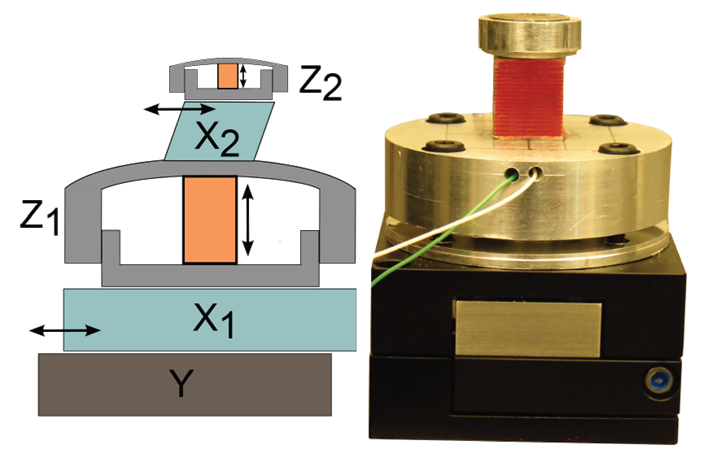
In this work we rely on design and control of serial kinematic nano-positioners containing multiple actuators. This enables us to simultaneously achieve high-speed, large kinematic range and nano-scale precision. The method benefits from an understanding of the dynamic coupling between various components of a positioner and the influence of the distribution of masses on control complexity. Our results show three orders of magnitude improvement in speed compared to conventional systems, while maintaining a large kinematic range. This is possible through a new control and mechanical design procedure to combine different actuators, some high-speed but short range while others featuring large-range but slow dynamics.
Real-time wide field nano-microscopy:
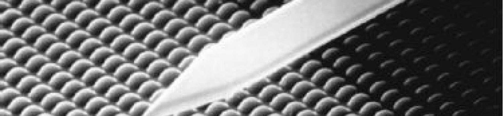
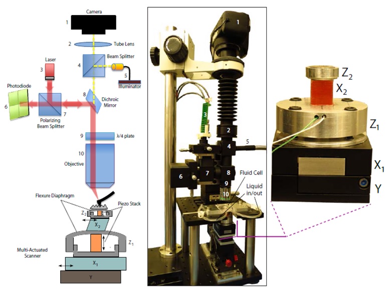
Conventional atomic force microscopes (AFM) are limited in speed and thus their applications are confined to the study of static samples. By enhancing several key AFM functionalities including optics, mechanical design, control, instrumentation and data acquisition, we have developed a real-time AFM, featuring a large-field of view. This instrument benefits from the nano-positioning system described earlier. The optics of the instrument includes RF modulation for reduced laser instability and accommodates ultra-small cantilevers (<10 µm long and <2 µm wide). From a design perspective, the instrument components are arranged modularly to enable easy exchange of the AFM components for different operating conditions such as imaging in liquid, air or vacuum under temperature or pressure constraints. The result is a modular AFM capable of capturing images at up to 10 frames per second. In the implemented setup the AFM has a field of view of 120 µm by 120 µm although, given the generality of the design methodology, the range can be further extended. The resulting AFM has been used to capture videos of nano-scale processes. Some of these videos have revealed vivid chemical and electrochemical phenomena that have never been seen before.
Some example videos of nano-scale processes taken by our modular high-speed large-range AFM setup.
Layer by layer etching of calcite in sulfuric acid.
Deposition/dissolution of copper on gold substrate.
Dissolution of calcite monolayers along the crystal lines